| CPC H01L 29/157 (2013.01) [H01L 21/02458 (2013.01); H01L 21/02507 (2013.01); H01L 21/0254 (2013.01); H01L 21/30625 (2013.01); H01L 29/2003 (2013.01); H01L 29/205 (2013.01); H01L 29/66462 (2013.01); H01L 29/7786 (2013.01)] | 16 Claims |
|
1. A semiconductor device, comprising:
a substrate;
a nucleation layer, disposed on the substrate;
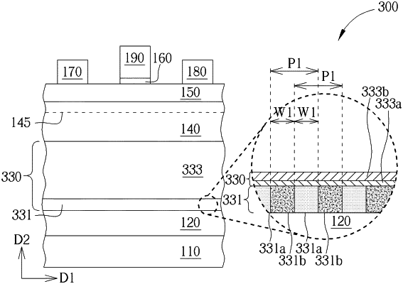
a buffer layer disposed on the nucleation layer, the buffer layer comprising:
a first superlattice layer, having at least two heteromaterials alternately arranged in a periodically ordered relation in a horizontal direction, wherein the first superlattice layer comprises a plurality of heterojunctions at interfaces between the at least two heteromaterials alternately arranged in the periodically ordered relation; and
a second superlattice layer, comprising a first material layer and a second material layer sequentially-stacked along a vertical direction, wherein each of the first material layer and the second material layer of the second superlattice layer consisted of a single material and simultaneously overlaps a whole top surface of the first superlattice layer, and the materials of the first material layer and the second material layer are different from each other;
an active layer disposed on the buffer layer; and
a gate electrode disposed on the active layer.
|