| CPC H01L 29/1095 (2013.01) [H01L 21/2253 (2013.01); H01L 21/2652 (2013.01); H01L 29/167 (2013.01); H01L 29/407 (2013.01); H01L 29/66734 (2013.01); H01L 29/7813 (2013.01)] | 20 Claims |

|
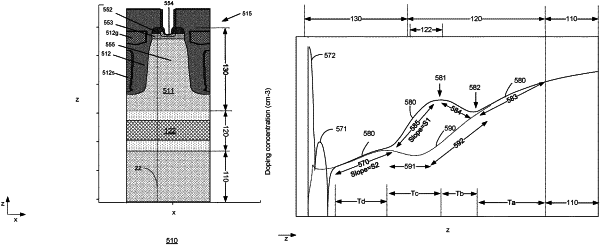
1. A method for preparing a substrate for fabricating a vertical MOSFET device, the method comprising:
forming a first epitaxial layer on a silicon wafer;
forming an ion-implanted capping layer in the first epitaxial layer; and
forming a device layer over the first epitaxial layer,
the silicon wafer being a phosphorus doped n+ silicon wafer, the first epitaxial layer being doped with phosphorus, the ion-implanted capping layer being an arsenic-implanted buried layer, and
wherein forming the device layer over the first epitaxial layer includes forming a source of the device in the device layer and forming a drain of the device in the silicon wafer.
|