| CPC H01L 29/0847 (2013.01) [H01L 21/02532 (2013.01); H01L 21/02535 (2013.01); H01L 21/30604 (2013.01); H01L 29/0673 (2013.01); H01L 29/1037 (2013.01); H01L 29/165 (2013.01); H01L 29/167 (2013.01); H01L 29/32 (2013.01); H01L 29/42392 (2013.01); H01L 29/66545 (2013.01); H01L 29/66795 (2013.01); H01L 29/785 (2013.01); H01L 21/0276 (2013.01); H01L 21/30625 (2013.01); H01L 22/26 (2013.01)] | 20 Claims |

|
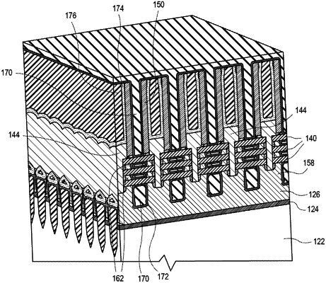
1. An integrated circuit structure, comprising:
a semiconductor fin;
a nanowire above the semiconductor fin;
a gate stack over the semiconductor fin and around the nanowire, the gate stack having a first side and a second side, the second side opposite the first side;
a first boron-doped germanium tin epitaxial source or drain structure on the semiconductor fin and at a first end of the nanowire, and adjacent to the first side of the gate stack; and
a second boron-doped germanium tin epitaxial source or drain structure on the semiconductor fin and at a first end of the nanowire and adjacent to the second side of the gate stack.
|