US 11,990,512 B2
Semiconductor device with doped structure
Miao-Syuan Fan, Hsinchu (TW); Pei-Wei Lee, Hsinchu (TW); Ching-Hua Lee, Hsinchu (TW); and Jung-Wei Lee, Hsinchu (TW)
Assigned to Taiwan Semiconductor Manufacturing Co., Ltd., Hsinchu (TW)
Filed by Taiwan Semiconductor Manufacturing Co., Ltd., Hsinchu (TW)
Filed on Feb. 14, 2022, as Appl. No. 17/650,867.
Application 17/650,867 is a continuation of application No. 16/937,365, filed on Jul. 23, 2020, granted, now 11,251,268.
Claims priority of provisional application 62/966,866, filed on Jan. 28, 2020.
Prior Publication US 2022/0165847 A1, May 26, 2022
This patent is subject to a terminal disclaimer.
Int. Cl. H01L 29/08 (2006.01); H01L 21/8234 (2006.01); H01L 27/088 (2006.01); H01L 29/10 (2006.01); H01L 29/40 (2006.01); H01L 29/417 (2006.01); H01L 29/423 (2006.01); H01L 29/66 (2006.01); H01L 29/78 (2006.01)
CPC H01L 29/0847 (2013.01) [H01L 21/823412 (2013.01); H01L 21/823418 (2013.01); H01L 21/823431 (2013.01); H01L 27/0886 (2013.01); H01L 29/1037 (2013.01); H01L 29/401 (2013.01); H01L 29/41791 (2013.01); H01L 29/42356 (2013.01); H01L 29/66795 (2013.01); H01L 29/785 (2013.01)] 20 Claims
OG exemplary drawing
 
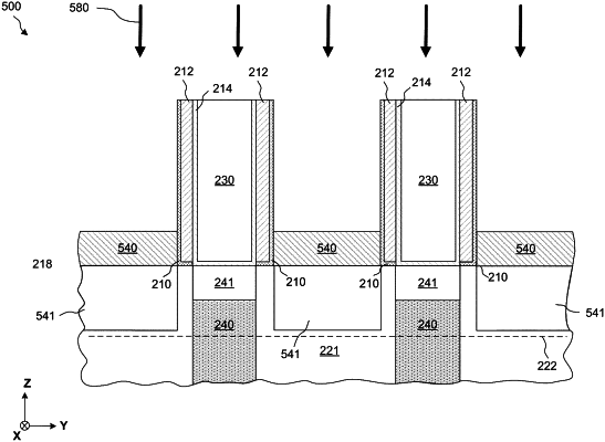
1. A method for forming a semiconductor device, comprising:
performing an ion implantation process on a substrate to form a first doped source/drain (S/D) region with a first concentration of lead (Pb) atoms;
performing an ion implantation process on the substrate to form a first doped channel region with a second concentration of Pb atoms, wherein the second concentration of Pb atoms is less than the first concentration of Pb atoms; and
performing a first treatment process on the doped S/D region.