| CPC H01L 29/0847 (2013.01) [H01L 29/24 (2013.01); H01L 21/02521 (2013.01); H01L 21/02529 (2013.01); H01L 21/0262 (2013.01); H01L 21/26513 (2013.01); H01L 29/7848 (2013.01); H01L 29/785 (2013.01)] | 20 Claims |
|
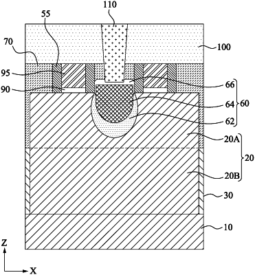
1. A semiconductor device, comprising:
a fin structure extending along a first direction having a channel region protruding from an isolation insulating layer;
a gate structure extending in a second direction disposed over the channel region and including a gate dielectric layer, a gate electrode layer and a sidewall spacer,
wherein the second direction is perpendicular to the first direction; and
a source/drain region adjacent to the channel region, wherein:
the source/drain region includes a first layer, a second layer formed on the first layer and a third layer formed on the second layer,
the first layer includes As,
the second layer includes SiP,
the third layer includes SiAs,
a bottom of the second layer is located below an upper surface of the isolation insulating layer, and
the first layer extends below the sidewall spacer along the first direction as viewed along a third direction perpendicular to the first and second directions.
|