| CPC H01L 29/0673 (2013.01) [H01L 21/0262 (2013.01); H01L 21/30604 (2013.01); H01L 21/31116 (2013.01); H01L 21/31155 (2013.01); H01L 29/66545 (2013.01); H01L 29/66795 (2013.01); H01L 29/785 (2013.01); H01L 21/26513 (2013.01); H01L 29/1083 (2013.01)] | 20 Claims |
|
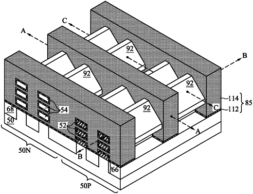
1. A structure comprising:
a nano-structure;
an epitaxial source/drain region adjacent the nano-structure;
a gate dielectric wrapped around the nano-structure;
a gate electrode over the gate dielectric, the gate electrode having an upper portion and a lower portion, a first width of the upper portion increasing continually in a first direction extending away from a top surface of the nano-structure, a second width of the lower portion being constant along the first direction; and
a gate spacer between the gate dielectric and the epitaxial source/drain region, the gate spacer having a first sidewall facing the epitaxial source/drain region and a second sidewall facing the gate dielectric, the first sidewall and the second sidewall of the gate spacer meeting at an apex.
|