US 11,990,508 B2
Dual step etch-back inner spacer formation
Andrew M. Greene, Slingerlands, NY (US); Yao Yao, Albany, NY (US); Ruilong Xie, Niskayuna, NY (US); and Veeraraghavan S. Basker, Schenectady, NY (US)
Assigned to INTERNATIONAL BUSINESS MACHINES CORPORATION, Armonk, NY (US)
Filed by INTERNATIONAL BUSINESS MACHINES CORPORATION, Armonk, NY (US)
Filed on Aug. 18, 2021, as Appl. No. 17/405,455.
Application 17/405,455 is a division of application No. 16/534,556, filed on Aug. 7, 2019, granted, now 11,139,372.
Prior Publication US 2021/0384296 A1, Dec. 9, 2021
Int. Cl. H01L 29/06 (2006.01); H01L 29/16 (2006.01); H01L 29/66 (2006.01); H01L 29/78 (2006.01)
CPC H01L 29/0669 (2013.01) [H01L 29/0653 (2013.01); H01L 29/16 (2013.01); H01L 29/66666 (2013.01); H01L 29/7827 (2013.01)] 20 Claims
OG exemplary drawing
 
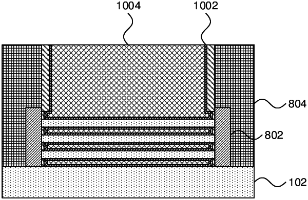
1. A semiconductor device, comprising:
a plurality of vertically stacked channel layers;
inner spacers between vertically adjacent pairs of the channel layer, each inner spacer having a middle portion that is thinner than a top and bottom portion; and
a gate stack formed over, around, and between the stacked channel layers.