| CPC H01L 29/0653 (2013.01) [H01L 29/1095 (2013.01); H01L 29/7816 (2013.01)] | 20 Claims |
|
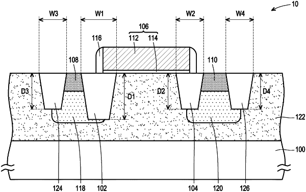
1. A high voltage transistor structure, comprising:
a substrate;
a first isolation structure and a second isolation structure disposed in the substrate;
a gate structure disposed on the substrate, at least a portion of the first isolation structure, and at least a portion of the second isolation structure;
a first source and drain region and a second source and drain region located in the substrate on two sides of the first isolation structure and the second isolation structure;
a first well region located in the substrate, wherein the first source and drain region is located in the first well region; and
a second well region located in the substrate, wherein the second source and drain region is located in the second well region, wherein
a depth of the first isolation structure is greater than a depth of the second isolation structure,
the gate structure is located directly above at least a portion of the first isolation structure and at least a portion of the second isolation structure, and
the first well region and the second well region are not located between the first isolation structure and the second isolation structure.
|