| CPC H01L 29/0649 (2013.01) [G11C 8/14 (2013.01); H10B 41/10 (2023.02); H10B 41/27 (2023.02); H10B 41/35 (2023.02); H10B 43/10 (2023.02); H10B 43/27 (2023.02); H10B 43/35 (2023.02)] | 20 Claims |
|
1. A three-dimensional (3D) memory device, comprising:
a substrate;
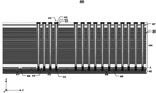
a memory stack on the substrate comprising a plurality of interleaved conductive layers and dielectric layers, an outmost one of the conductive layers toward the substrate being a source select gate line (SSG);
a plurality of channel structures each extending vertically through the memory stack; and
one or more isolation structures each surrounding at least one of the channel structures in a plan view to separate the SSG and the at least one channel structure,
wherein a first group of the plurality of channel structures is spaced apart from the SSG and a second group of the plurality of channel structures is in direct contact with the SSG.
|