| CPC H01L 29/0615 (2013.01) [H01L 29/0646 (2013.01); H01L 29/1058 (2013.01); H01L 29/66833 (2013.01)] | 7 Claims |
|
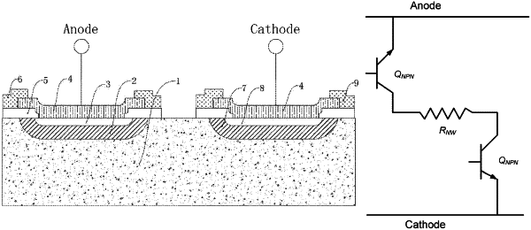
1. A transient-voltage-suppression protection device, comprising: a substrate, a first trap, a second trap, a first injection region, and a second injection region, and two open-base triodes with a common collector connected in series and provided symmetrically, wherein the two open-base triodes share a same substrate;
one of the two open-base triodes comprises the first trap and the first injection region provided on the first trap;
another of the two open-base triodes comprises the second trap and the second injection region provided on the second trap;
the first trap and the second trap are sequentially arranged on the substrate from left to right at an interval, have a same doping type that is opposite to a doping type of the substrate, and the first injection region and the second injection region have opposite doping types;
the substrate serves as a common collector, the first trap and the second trap serve as bases respectively, and the first injection region and the second injection region are respectively connected via a metal and led out as emitters;
a PN junction formed between the first trap and the substrate has the same junction depth as a PN junction formed between the second trap and the substrate, and a PN junction formed between the first injection region and the first trap has the same junction depth as a PN junction formed between the second injection region and the second trap, doping concentrations of the first trap, the first injection region and the substrate increase sequentially, doping concentrations of the second trap, and the second injection region and the substrate increase sequentially;
the first trap and the second trap have a same doping concentration, and the first injection region and the second injection region have a same doping concentration;
the first injection region and the second injection region are arranged at central positions of the first trap and the second trap respectively;
there is a spacing distance of 5-20 μm between the first trap and the second trap; and
the substrate as the collector has a resistivity of 30-1500 Ω·cm.
|