| CPC H01L 28/75 (2013.01) [H01L 23/5223 (2013.01)] | 5 Claims |
|
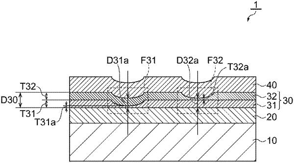
1. A capacitor having an MIM, comprising:
a lower electrode;
an upper electrode; and
dielectric layers laminated on an upper surface of the lower electrode from the lower electrode to the upper electrode to form a dielectric for the capacitor;
wherein the dielectric layers include a first dielectric layer having a first thickness on an upper surface of the lower electrode, and a second dielectric layer having a second thickness on an upper surface of the first dielectric layer and being in contact with the upper electrode,
wherein, in plan view of the capacitor, the dielectric has a first defect portion and a second defect portion at different locations,
wherein the first defect portion is a depression at the upper surface of the first dielectric layer and does not go through the first dielectric layer to the lower electrode, and
wherein the second defect portion is a depression at the upper surface of the second dielectric layer and does not go through the second dielectric layer to the first dielectric layer.
|