US 11,990,503 B2
Methods of fabricating capacitor and semiconductor device including the capacitor
Gabjin Nam, Seoul (KR); Youngbin Lee, Suwon-si (KR); Cheoljin Cho, Hwaseong-si (KR); and Jaehyoung Choi, Hwaseong-si (KR)
Assigned to SAMSUNG ELECTRONICS CO., LTD., Suwon-si (KR)
Filed by SAMSUNG ELECTRONICS CO., LTD., Suwon-si (KR)
Filed on Jul. 15, 2021, as Appl. No. 17/376,458.
Claims priority of application No. 10-2021-0001055 (KR), filed on Jan. 5, 2021.
Prior Publication US 2022/0216296 A1, Jul. 7, 2022
Int. Cl. H10B 53/30 (2023.01); G11C 11/22 (2006.01); H01L 49/02 (2006.01)
CPC H01L 28/60 (2013.01) [H10B 53/30 (2023.02); G11C 11/22 (2013.01); H01L 28/55 (2013.01)] 20 Claims
OG exemplary drawing
 
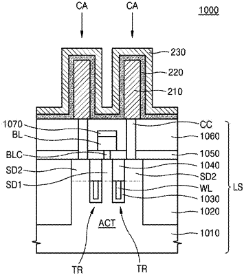
1. A method of fabricating a capacitor, the method comprising:
forming a first electrode;
forming a dielectric layer on the first electrode;
forming a second electrode on the dielectric layer; and
applying, between the first electrode and the second electrode, a voltage outside an operating voltage range applied during operation or a current outside an operating current range applied during operation.