| CPC H10K 59/1213 (2023.02) [G09G 3/3275 (2013.01); H10K 50/11 (2023.02); H10K 59/1216 (2023.02); H10K 59/131 (2023.02); G09G 2300/0857 (2013.01); G09G 2310/0251 (2013.01); G09G 2310/0262 (2013.01)] | 6 Claims |
|
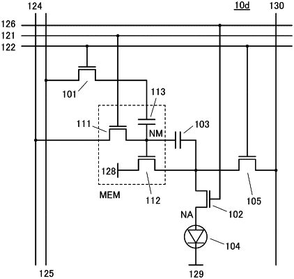
1. A display device comprising a pixel, the pixel comprising:
a first transistor, a second transistor, a third transistor, a fourth transistor, a fifth transistor, a first capacitor, a second capacitor, and a display element,
wherein one of a source and a drain of the first transistor is electrically connected to a first electrode of the first capacitor,
wherein a second electrode of the first capacitor is electrically connected to one of a source and a drain of the second transistor, a gate of the third transistor, and a first electrode of the second capacitor,
wherein a second electrode of the second capacitor is electrically connected to one of a source and a drain of the third transistor, one of a source and a drain of the fourth transistor, and one of a source and a drain of the fifth transistor,
wherein the second electrode of the second capacitor is electrically connected to the display element through the fourth transistor,
wherein another one of the source and the drain of the fourth transistor is electrically connected to the display element,
wherein another one of the source and the drain of the first transistor is electrically connected to a first wiring that supplies first data,
wherein another one of the source and the drain of the second transistor is electrically connected to a second wiring that supplies second data,
wherein another one of the source and the drain of the third transistor is electrically connected to a third wiring which is a power supply line,
wherein the first electrode of the first capacitor is not electrically connected to the second electrode of the second capacitor,
wherein another one of the source and the drain of the fifth transistor is electrically connected to a fourth wiring,
wherein a gate of the first transistor is electrically connected to a first scan line,
wherein a gate of the second transistor is electrically connected to a second scan line,
wherein a gate of the fourth transistor is electrically connected to a third scan line, and
wherein a gate of the fifth transistor is electrically connected to the first scan line.
|