| CPC H01L 27/156 (2013.01) [G09G 3/32 (2013.01); H01L 33/005 (2013.01); H01L 33/38 (2013.01); H01L 33/62 (2013.01); H01L 2933/0016 (2013.01); H01L 2933/0066 (2013.01)] | 16 Claims |

|
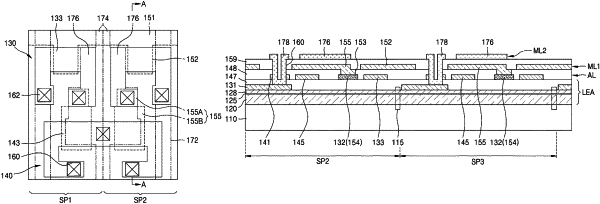
1. A micro light emitting display apparatus, comprising:
a micro light emitting element;
a driving transistor connected to the micro light emitting element;
a switching transistor connected to the driving transistor;
a capacitor connected to the driving transistor and the switching transistor;
a first opening provided to expose a source region or a drain region of the switching transistor;
a gate electrode of the driving transistor provided in the first opening, and in contact with the source region or the drain region of the switching transistor,
an anode electrode provided on the micro light emitting element;
a second opening provided to expose the anode electrode; and
a metal line provided in the second opening,
wherein a first end of the gate electrode of the driving transistor is provided on a source region or a drain region of the driving transistor and a second end of the gate electrode of the driving transistor is provided to physically contact the source region or the drain region of the switching transistor, and
wherein the second opening is configured to penetrate a drain region of the driving transistor.
|