| CPC H01L 27/14669 (2013.01) [B81C 1/00 (2013.01); B81C 1/00246 (2013.01); G01J 5/0225 (2013.01); G01J 5/024 (2013.01); G01J 5/046 (2013.01); G01J 5/048 (2013.01); G01J 5/0853 (2013.01); G01J 5/12 (2013.01); G01J 5/16 (2013.01); H01L 27/146 (2013.01); H01L 27/14612 (2013.01); H01L 27/14629 (2013.01); H01L 27/14643 (2013.01); H01L 27/14649 (2013.01); H01L 31/0224 (2013.01); H01L 31/09 (2013.01); B81C 2203/0742 (2013.01); G01J 2005/123 (2013.01)] | 19 Claims |
|
1. A device comprising:
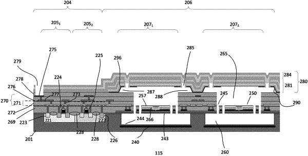
a substrate prepared with a complementary metal oxide semiconductor (CMOS) region with CMOS devices and a sensor region with micro-electro-mechanical system (MEMS) region with a MEMS component, wherein the MEMS component comprises a thermoelectric IR sensor; and
a CMOS compatible cap disposed on the substrate over the CMOS region and MEMS region, wherein the CMOS compatible cap includes CMOS layers, the CMOS compatible cap comprises
a first cap portion disposed over the MEMS region,
a second cap portion disposed over the CMOS region, and
wherein the first cap portion over the MEMS region is elevated above the second cap portion over the CMOS region to create a cap cavity over the MEMS region.
|
|
2. The device of claim 1 wherein the MEMS component comprises an array of thermoelectric IR sensor cells.
|
|
15. A device comprising:
a substrate prepared with a complementary metal oxide semiconductor (CMOS) region with CMOS devices and a sensor region with micro-electro-mechanical system (MEMS) region with a MEMS component, wherein the MEMS component comprises a thermoelectric IR sensor; and
a CMOS compatible cap disposed on the substrate over the CMOS region and MEMS region, wherein the CMOS compatible cap includes CMOS layers, the CMOS compatible cap is elevated over the MEMS region to provide a cap cavity between the CMOS compatible cap and the MEMS region, wherein a bottom surface of the CMOS compatible cap above the MEMS device region is non-planar, the bottom surface of the CMOS compatible cap includes a depression above the MEMS device region, the CMOS compatible cap comprises
a base cap having a CMOS IR transparent base cap layer, the base cap includes a cap release opening, and
a seal cap for sealing the cap release opening in the base cap.
|
|
16. A device comprising:
a substrate prepared with a complementary metal oxide semiconductor (CMOS) region with CMOS devices and a sensor region with micro-electro-mechanical system (MEMS) region with a MEMS component;
a CMOS compatible IR transparent cap disposed on the substrate over the CMOS region and MEMS region, wherein the CMOS IR transparent compatible cap includes CMOS layers, the CMOS compatible cap is elevated over the MEMS region to provide a cap cavity between the CMOS compatible cap and the MEMS region;
an interlevel dielectric (ILD) layer disposed on the substrate over the CMOS region and MEMS region, covering the CMOS devices and MEMS component, the ILD layer includes ILD contacts coupled to contact regions of the CMOS devices;
a back-end-of-line (BEOL) dielectric is disposed on the ILD layer, the BEOL dielectric includes a plurality of intermetal dielectric (IMD) levels, wherein an IMD level includes a metal level with metal lines and a via level thereover with via contacts; and
a passivation layer disposed over a top metal level of the BEOL dielectric.
|