| CPC H01L 27/14641 (2013.01) [H01L 27/14612 (2013.01); H01L 27/14806 (2013.01); H04N 25/633 (2023.01)] | 18 Claims |

|
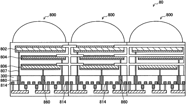
1. A solid-state imaging element, comprising:
a semiconductor substrate;
a first photoelectric conversion unit above the semiconductor substrate and configured to convert light into a charge; and
a second photoelectric conversion unit above the first photoelectric conversion unit and configured to convert light into a charge, wherein
the first photoelectric conversion unit and the second photoelectric conversion unit are joined at joint surfaces that face each other,
each of the first photoelectric conversion unit and the second photoelectric conversion unit has
a laminated structure including:
an upper electrode;
a lower electrode;
a photoelectric conversion film sandwiched between the upper electrode and the lower electrode; and
a storage electrode opposed to the upper electrode via the photoelectric conversion film and a first insulating film,
the lower electrode of the first photoelectric conversion unit is
electrically connected to a charge storage unit in the semiconductor substrate, via a first through electrode that penetrates the semiconductor substrate,
the lower electrode of the second photoelectric conversion unit is
electrically connected to the charge storage unit via:
a second electrode on a joint surface of the second photoelectric conversion unit;
a first electrode on a joint surface of the first photoelectric conversion unit so as to be opposed to the second electrode and joined to the second electrode;
a second through electrode that penetrates the first photoelectric conversion unit; and
the first through electrode.
|