| CPC H01L 27/14638 (2013.01) [H01L 27/1463 (2013.01)] | 16 Claims |
|
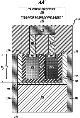
1. A pixel, comprising:
a photodiode formed in a semiconductor substrate and having a photodiode doped region with a PD dopant concentration, wherein the photodiode has a first conductive type, wherein the semiconductor substrate has a second conductive type opposite to the first conductive type;
a floating diffusion formed in the semiconductor substrate and having an FD dopant concentration of the first conductive type, wherein the FD dopant concentration is higher than the PD dopant concentration; and
a transfer structure selectively coupling the photodiode to the floating diffusion, wherein the transfer structure comprises:
a transfer gate formed on the semiconductor substrate; and
a vertical channel structure comprising spaced apart first doped regions formed in the semiconductor substrate between the transfer gate and the photodiode, wherein each spaced apart first doped region is doped at a first dopant concentration with a first-type dopant of the second conductive type, wherein the spaced apart first doped regions are formed in a second doped region doped at a second dopant concentration with a second-type dopant of the first conductive type, wherein the second dopant concentration is greater than the PD dopant concentration, less than the first dopant concentration, and less than the FD dopant concentration.
|