| CPC H01L 27/14636 (2013.01) [H01L 27/14618 (2013.01); H01L 27/14683 (2013.01)] | 16 Claims |
|
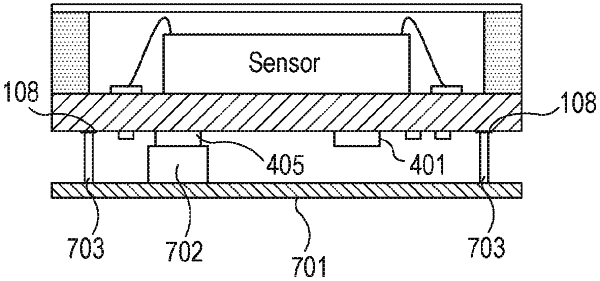
1. An image capturing unit comprising a semiconductor chip constituting an image sensor and a substrate on which the semiconductor chip is mounted, the image capturing unit comprising:
a plurality of input wiring lines for controlling the semiconductor chip;
a plurality of first electrodes connecting to the input wiring lines; and
an input connector connecting to the input wiring lines,
wherein the substrate includes a first area and a second area on a first surface opposite to a second surface on which the semiconductor chip is mounted,
wherein the input connector and an electronic component are disposed in the first area, and at least one or more of the plurality of first electrodes are disposed in the second area, and
wherein the semiconductor chip can be driven via the plurality of first electrodes.
|