| CPC H01L 27/14634 (2013.01) [H01L 27/14618 (2013.01); H01L 27/1462 (2013.01); H01L 27/14632 (2013.01); H01L 27/14636 (2013.01); H01L 27/14643 (2013.01); H01L 27/14685 (2013.01); H01L 27/14687 (2013.01); H01L 27/14689 (2013.01); H01L 27/1469 (2013.01)] | 5 Claims |
|
1. A package structure, comprising:
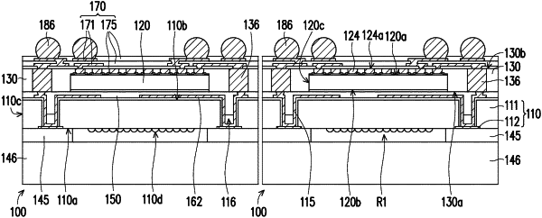
a first die, comprising a silicon substrate and a die pad, wherein the first die has a first active surface and a first back surface opposite to the first active surface, wherein the first active surface has a sensing area, the die pad is located on the active surface;
a second die, comprising a second active surface and a second back surface opposite to the second active surface, wherein the second die is arranged such that the second back surface faces the first back surface of the first die;
an encapsulant, covering the second die and having a first encapsulating surface and a second encapsulating surface opposite to the first encapsulating surface;
a dam structure, located on the first encapsulating surface and exposing the sensing area of the first die;
a light-transmitting sheet, located on the dam structure;
a conductive connector, penetrating the encapsulant;
a first circuit layer, located on the second encapsulating surface;
an insulating layer, located on the first back surface of the first die and extendedly penetrating the silicon substrate to directly cover a portion of the die pad;
a conductive layer, located on the insulating layer and extendedly penetrating the silicon substrate to in contact with a portion of the die pad exposed by the insulating layer,
wherein a portion of the conductive layer located on the first back surface of the first die forms a second circuit layer located on the first encapsulating surface,
wherein a portion of the insulating layer penetrating the silicon substrate and a portion of the conductive layer penetrating the silicon substrate forms a through silicon,
wherein the die pad of the first die is electrically connected to the second die through the through silicon via, the second circuit layer, the conductive connector and the first circuit layer;
a dielectric layer, located on the second circuit layer and covering the through silicon via,
wherein a portion of the dielectric layer is embedded in the silicon substrate,
wherein the portion of the dielectric layer embedded in the silicon substrate and the portion of the conductive layer forming the through silicon via form a gas gap; and
a conductive terminal, disposed on the first circuit layer.
|