| CPC H01L 27/14629 (2013.01) [H01L 27/14621 (2013.01); H01L 27/1463 (2013.01); H01L 27/14645 (2013.01); H01L 27/14685 (2013.01)] | 20 Claims |
|
1. An image sensor device, comprising:
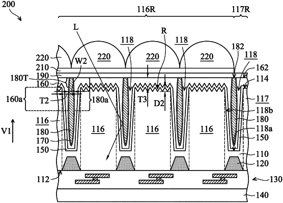
a semiconductor substrate having a front surface, a back surface opposite to the front surface, and a light-sensing region close to the front surface;
an insulating layer covering the back surface and extending into the semiconductor substrate, wherein the insulating layer surrounds the light-sensing region, and a thickness of an upper portion of the insulating layer in the semiconductor substrate increases in a direction away from the front surface;
a protection layer between the insulating layer and the semiconductor substrate, wherein the protection layer has a first refractive index, and the first refractive index is less than a second refractive index of the semiconductor substrate and greater than a third refractive index of the insulating layer, and the protection layer conformally and continuously covers the back surface and extends into the semiconductor substrate; and
a reflective structure surrounded by insulating layer in the semiconductor substrate, wherein the reflective structure has a first end and a second end, the second end is between the first end and the front surface, and a middle portion of the reflective structure is wider than the first end or the second end.
|