| CPC H01L 27/14623 (2013.01) [H01L 27/14605 (2013.01); H01L 27/14692 (2013.01); H04N 25/60 (2023.01); H04N 25/702 (2023.01)] | 18 Claims |
|
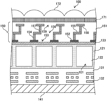
1. An imaging device, comprising:
a plurality of photoelectric converters on a semiconductor substrate, wherein each of the plurality of photoelectric converters is configured to perform photoelectric conversion according to incident light;
a light path portion that includes:
a transparent film through which the incident light is transmissible;
a first light-blocking wall for each of the plurality of photoelectric converters, wherein
the first light-blocking wall partitions the transparent film in a direction perpendicular to the semiconductor substrate, and
the first light-blocking wall is configured to block the incident light;
a light-blocking film at a first end of the first light-blocking wall, wherein
the first end is opposite to a second end of the first light-blocking wall that is closer to the semiconductor substrate,
the light-blocking film has a length parallel to the semiconductor substrate, and
the light-blocking film includes, for each of the plurality of photoelectric converters, an opening through which the incident light is transmissible; and
a second light-blocking wall configured to block the incident light, wherein
the light-blocking film is between the first light-blocking wall and the second light-blocking wall, and
the first light-blocking wall and the second light-blocking wall are at opposite ends of the light-blocking film in a direction parallel to the semiconductor substrate; and
an on-chip lens that corresponds to each of the plurality of photoelectric converters, wherein the on-chip lens is configured to collect the incident light into a photoelectric converter of the plurality of photoelectric converters through the light path portion.
|