| CPC H01L 27/14621 (2013.01) [H01L 27/14609 (2013.01); H01L 27/1463 (2013.01); H04N 25/77 (2023.01); H01L 27/14627 (2013.01)] | 20 Claims |
|
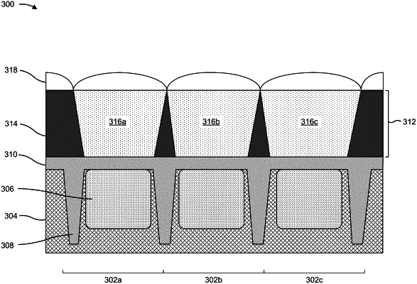
1. A pixel sensor, comprising:
a photodiode in a substrate;
an isolation structure, in the substrate, comprising trenches extending around perimeters of the pixel sensor and from a top surface of the substrate to a depth, in the substrate, deeper than the photodiode;
a grid structure, above the photodiode, comprising sidewalls over the trenches of the isolation structure;
a color filter region over the photodiode and in between the sidewalls of the grid structure,
wherein the sidewalls of the grid structure include a first sidewall angled from a first point on a bottom surface of the color filter region to a first point on a top surface of the color filter region, and a second sidewall angled from a second point on the bottom surface of the color filter region to a second point on the top surface of the color filter region; and
a micro-lens layer comprising a micro-lens having a first end, on the first point of the top surface of the color filter region, and a second end, on the second point of the top surface of the color filter region.
|