| CPC H01L 27/14605 (2013.01) [B60R 1/001 (2013.01); G02B 23/2407 (2013.01); H01L 27/14621 (2013.01); H04N 25/766 (2023.01); H04N 23/555 (2023.01)] | 9 Claims |
|
1. A solid-state imaging device, comprising:
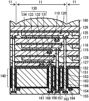
a stacked photoelectric converter for each of a plurality of pixels, the stacked photoelectric converter having a plurality of photoelectric conversion elements stacked therein, the plurality of photoelectric conversion elements each having different wavelength selectivity; and
a plurality of first pixel circuits, wherein one first pixel circuit is provided for each of a plurality of groups, each first pixel circuit outputting a pixel signal based on an electric charge outputted from a corresponding one of a plurality of first photoelectric conversion elements of a plurality of the photoelectric conversion elements, each of the first photoelectric conversion elements having predetermined wavelength selectivity, the groups being obtained by dividing the plurality of the first photoelectric conversion elements into the plurality of groups, wherein
the solid-state imaging device further includes a plurality of drive wiring lines to which control signals are applied, the control signals being for controlling output of electric charges accumulated in the photoelectric conversion elements, and
each of the drive wiring lines is coupled to the first photoelectric conversion elements belonging to a first group and the first photoelectric conversion elements belonging to a second group in each of a plurality of unit pixel columns corresponding to shared first pixel circuits, the plurality of the first photoelectric conversion elements belonging to the first group and the plurality of the first photoelectric conversion elements belonging to the second group sharing the different first pixel circuits.
|