| CPC H01L 27/14603 (2013.01) [H01L 27/14638 (2013.01); H01L 27/14683 (2013.01)] | 31 Claims |

|
1. A photoelectric conversion device comprising:
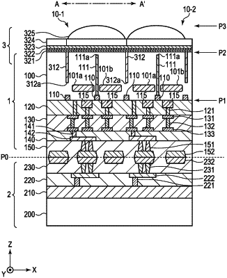
a semiconductor substrate having a first face and a second face that is arranged on an opposite side of the first face and receives light, and including a first photoelectric conversion portion, a second photoelectric conversion portion, and a third photoelectric conversion portion, wherein the first photoelectric conversion portion, the second photoelectric conversion portion, and the third photoelectric conversion portion are arranged in this order in a horizontal direction of the substrate,
wherein the semiconductor substrate includes:
a first trench extending from the first face between the first photoelectric conversion portion and the second photoelectric conversion portion,
a first insulating layer arranged in the first trench,
a second trench extending from the second face between the second photoelectric portion and the third photoelectric portion, and
a second insulating layer arranged in the second trench,
wherein, along a direction from the first face to the second face, the first insulating layer and another part of the semiconductor substrate are arranged in this order, and a part of the semiconductor substrate and the second insulating layer arranged in this order,
wherein an end on a second face side of the first trench is located closer to the second face than an end on a first face side of the second trench, and
wherein the first trench has a first portion extending from the first face toward the second face, and a second portion extending from a bottom surface of the first portion toward the second face, and a maximum width of the second portion is smaller than a minimum width of the first portion in a cross section taken along a direction in which the first photoelectric conversion portion and the second photoelectric conversion portion are arranged.
|