| CPC H01L 27/1248 (2013.01) [H01L 27/1259 (2013.01)] | 20 Claims |
|
1. An array substrate, comprising:
an underlay;
an active layer disposed on the underlay;
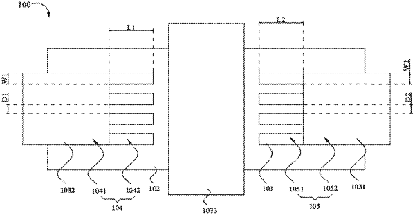
a gate electrode insulation layer, wherein the gate electrode insulation layer is disposed on the active layer and covers the active layer, the gate electrode insulation layer comprises a first through hole set and a second through hole set disposed oppositely; wherein the first through hole set comprises a first through hole and second through holes, the second through holes are defined in a side of the first through hole set near the second through hole set, the second through hole set comprises third through holes and a fourth through hole, the third through holes are defined in a side of the second through hole set near the first through hole set, and the second through holes and the third through holes each include a plurality of holes; and
a metal layer disposed on the gate electrode insulation layer, wherein the metal layer comprises a source electrode, a drain electrode, and a gate electrode, the drain electrode is connected to the active layer through the first through hole, and the source electrode is connected to the active layer through the fourth through hole.
|