| CPC H01L 27/1244 (2013.01) | 20 Claims |
|
1. An array substrate, comprising:
a substrate;
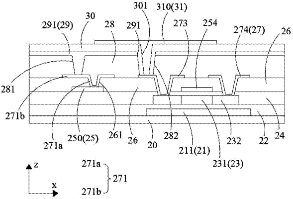
a first metal layer disposed on the substrate and comprising a plurality of common signal lines;
a first insulating layer covering the first metal layer and provided with a plurality of first via holes;
a second metal layer disposed on a side of the first insulating layer away from the first metal layer and comprising a plurality of conductive electrodes, wherein the conductive electrodes are connected to the common signal lines through the first via holes;
a second insulating layer disposed on the side of the first insulating layer away from the first metal layer and covering the second metal layer, and a plurality of second via holes defined on the second insulating layer;
a first electrode layer disposed on a side of the second insulating layer away from the second metal layer and comprising a plurality of first electrodes, wherein the first electrodes are connected to the conductive electrodes through the second via holes;
a second electrode layer disposed on a side of the first electrode layer away from the second insulating layer and comprising a plurality of second electrodes;
wherein an orthographic projection of at least one of the second via hole or the second electrode on the substrate is staggered from an orthographic projection of the first via hole on the substrate.
|