| CPC H01L 27/124 (2013.01) [G02F 1/133603 (2013.01); H01L 25/0753 (2013.01); H01L 27/127 (2013.01); H01L 27/156 (2013.01); H01L 33/62 (2013.01); H01L 2933/0066 (2013.01)] | 12 Claims |
|
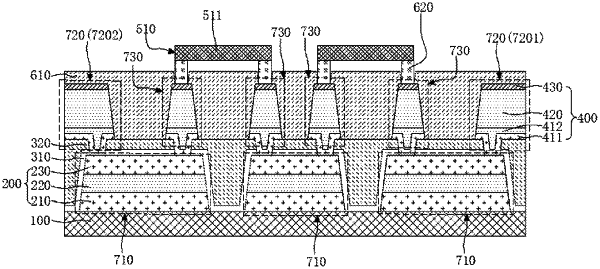
1. An array substrate, comprising:
a base substrate;
a metal wiring layer provided on a side of the base substrate and comprising a first copper metal layer;
a planarization layer provided on a side of the metal wiring layer away from the base substrate;
a drive lead layer provided on a side of the planarization layer away from the base substrate, wherein the drive lead layer is electrically connected to the metal wiring layer, the drive lead layer comprises a second copper metal layer, and a thickness of the second copper metal layer is greater than a thickness of the first copper metal layer; and
a functional device layer provided on a side of the drive lead layer away from the base substrate, wherein the functional device layer is electrically connected to the metal wiring layer or the drive lead layer.
|