| CPC H01L 27/124 (2013.01) [H01L 25/167 (2013.01); H01L 27/1248 (2013.01)] | 8 Claims |
|
1. A display device comprising:
a substrate;
a plurality of pixels provided to the substrate;
a light emitting element and a plurality of transistors provided to each of the pixels;
a plurality of signal lines configured to supply a signal to the pixels;
a power supply line configured to supply a drive potential to the pixels;
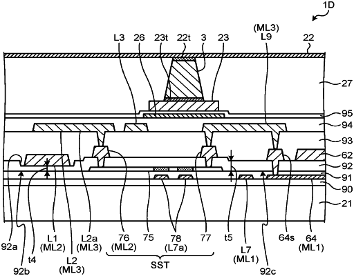
a first metal layer, a second metal layer, and a third metal layer provided in different layers in a first direction perpendicular to the substrate;
a first insulating film provided between the first metal layer and the second metal layer; and
a second insulating film provided between the second metal layer and the third metal layer,
wherein
the transistors each comprise:
a semiconductor layer provided to the substrate; and
a gate electrode formed in the first metal layer and provided in a region overlapping the semiconductor layer,
the signal lines are formed in the third metal layer and electrically coupled to the transistors,
the power supply line is formed in the second metal layer,
the power supply line overlaps at least one of the signal lines in planar view,
the first insulating film includes a first part overlapping the power supply line and a second part not overlapping the power supply line,
the thickness of the first part is smaller than the thickness of the second part,
an upper surface of the first part is closer to the substrate than an upper surface of the second part, in the first direction, and
relative permittivity of the first insulating film is higher than relative permittivity of the second insulating film.
|