| CPC H01L 27/1211 (2013.01) [H01L 27/0207 (2013.01); H01L 29/41791 (2013.01); H01L 29/66795 (2013.01); H01L 29/785 (2013.01)] | 20 Claims |

|
1. A method of fabricating a circuit cell, comprising:
accessing a logic design for implementing a function of the circuit cell, the logic design including a plurality of logic components;
accessing a plurality of circuit structures for implementing one or more of the logic components, the plurality of circuit structures including,
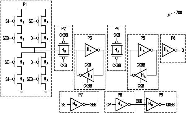
a first circuit structure comprising a first circuit component that includes fin field-effect transistors (finFETs) formed in a first fin portion of the circuit cell, the first fin portion including a plurality of first fin structures arranged in first rows, and
a second circuit structure comprising a second circuit component that includes finFETs formed in a second fin portion of the circuit cell, the second fin portion of the circuit including a plurality of second fin structures arranged in a plurality of second rows, wherein each of the second rows, in the second fin portion, contain a lesser number of fin structures than each of the first rows, in the first fin portion of the circuit cell;
generating a plurality of circuit designs that use different combinations of the plurality of circuit structures that implement the function;
filtering the generated circuit designs that do not meet a first circuit criterion; and
selecting a remaining circuit design that has an optimum value for a second circuit criterion.
|