| CPC H01L 27/0922 (2013.01) [H01L 21/02 (2013.01); H01L 21/8238 (2013.01); H01L 21/823807 (2013.01); H01L 21/8258 (2013.01); H01L 27/0924 (2013.01); H01L 27/1211 (2013.01); H01L 29/045 (2013.01); H01L 29/06 (2013.01); H01L 29/78 (2013.01); H01L 21/02609 (2013.01)] | 20 Claims |
|
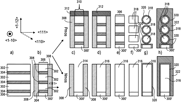
1. An integrated circuit structure, comprising:
a plurality of vertically stacked silicon nanowires disposed above a substrate, each of the silicon nanowires comprising a discrete channel region having <111> lateral sidewalls along a <110> carrier transport direction, wherein the <111> lateral sidewalls are substantially vertical sidewalls;
a common P-type gate electrode stack surrounding each of the discrete channel regions of the plurality of vertically stacked silicon nanowires;
a pair of dielectric spacers on either side of the common P-type gate electrode stack, each of the pair of dielectric spacers comprising a continuous material disposed along a sidewall of the common P-type gate electrode and surrounding a discrete portion of each of the vertically stacked silicon nanowires; and
a pair of source and drain regions on either side of the pair of dielectric spacers.
|