| CPC H01L 27/0922 (2013.01) [H01L 21/823814 (2013.01); H01L 21/823892 (2013.01); H01L 27/0207 (2013.01); H01L 27/092 (2013.01); H01L 27/0925 (2013.01); H01L 25/0657 (2013.01); H01L 2225/06524 (2013.01)] | 19 Claims |
|
1. A semiconductor device comprising:
a substrate;
an N-well area formed in the substrate;
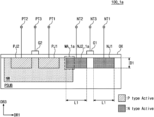
a first P-channel metal oxide semiconductor (PMOS) transistor having active regions formed in the N-well area; and
a first N-channel metal oxide semiconductor (NMOS) transistor having active regions formed in the substrate,
wherein the first NMOS transistor includes a first N-type active region overlapping each of the substrate and the N-well area, when viewed from above a plane parallel to a top surface of the substrate, and
wherein a first portion of the first N-type active region overlaps the N-well area from above the plane and is a well guard-ring of the N-well area.
|