| CPC H01L 27/0886 (2013.01) [H01L 21/823807 (2013.01); H01L 21/823821 (2013.01); H01L 21/823871 (2013.01); H01L 21/823878 (2013.01); H01L 27/0207 (2013.01); H01L 27/092 (2013.01); H01L 27/0924 (2013.01); H01L 29/1041 (2013.01); H01L 29/7835 (2013.01); H01L 29/785 (2013.01); H01L 21/823814 (2013.01); H03K 3/0315 (2013.01)] | 20 Claims |
|
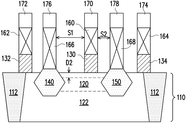
1. A method of fabricating a semiconductor device, the method comprising:
forming a gate structure, a first edge structure and a second edge structure on a semiconductor strip;
forming a first source/drain feature between the gate structure and the first edge structure;
forming a second source/drain feature between the gate structure and the second edge structure, wherein a distance between the gate structure and the first source/drain feature is different from a distance between the gate structure and the second source/drain feature; and
implanting a buried channel in the semiconductor strip, wherein the buried channel is entirely below a top-most surface of the semiconductor strip, a maximum depth of the buried channel is less than a maximum depth of the first source/drain feature, and a dopant concentration of the buried channel is highest under the gate structure.
|