| CPC H01L 27/0886 (2013.01) [H01L 21/823431 (2013.01); H01L 21/823462 (2013.01); H01L 29/517 (2013.01); H01L 29/66795 (2013.01); H01L 29/785 (2013.01)] | 17 Claims |
|
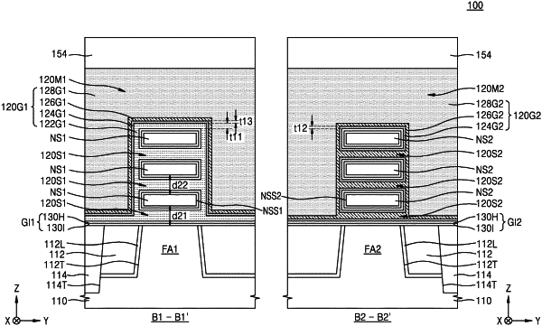
1. An integrated circuit device comprising:
a substrate including a first fin-type active region and a second fin-type active region spaced apart from the first fin-type active region in a first direction;
a plurality of first semiconductor patterns on the first fin-type active region and being spaced apart from each other in a vertical direction;
a plurality of second semiconductor patterns on the second fin-type active region and being spaced apart from each other in the vertical direction; and
a gate structure on the first and second fin-type active regions and extending in the first direction, the gate structure including:
a first conductive layer surrounding each of the plurality of first semiconductor patterns and filling a first sub-gate space between the respective first semiconductor patterns;
a second conductive layer on the first conductive layer and surrounding each of the plurality of second semiconductor patterns, the second conductive layer covering the plurality of first semiconductor patterns, but not disposed in the first sub-gate space;
a third conductive layer on the second conductive layer and filling a second sub-gate space between each of the plurality of second semiconductor patterns, the third conductive layer covering the plurality of first semiconductor patterns, but not disposed in the first sub-gate space; and
a buried conductive layer on the third conductive layer.
|