| CPC H01L 27/0886 (2013.01) [G11C 5/06 (2013.01); H01L 27/0688 (2013.01); H01L 29/0669 (2013.01); H01L 29/41791 (2013.01); H01L 29/66795 (2013.01); H01L 29/785 (2013.01); H01L 2029/7858 (2013.01)] | 11 Claims |
|
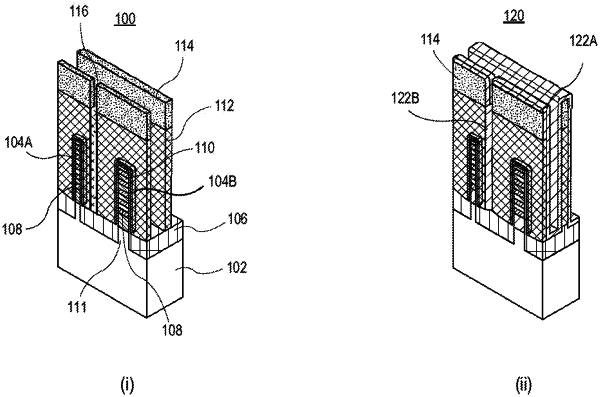
1. An integrated circuit structure, comprising:
a first vertical arrangement of horizontal nanowires;
a second vertical arrangement of horizontal nanowires;
a first gate stack over the first vertical arrangement of horizontal nanowires;
a second gate stack over the second vertical arrangement of horizontal nanowires, an end of the second gate stack spaced apart from an end of the first gate stack by a gap; and
a dielectric structure comprising a first portion forming a gate spacer along sidewalls of the first gate stack, a second portion forming a gate spacer along sidewalls of the second gate stack, and a third portion completely filling the gap, the third portion continuous with the first and second portions.
|