| CPC H01L 27/088 (2013.01) [H01L 21/76224 (2013.01); H01L 29/42392 (2013.01); H01L 29/78696 (2013.01)] | 20 Claims |
|
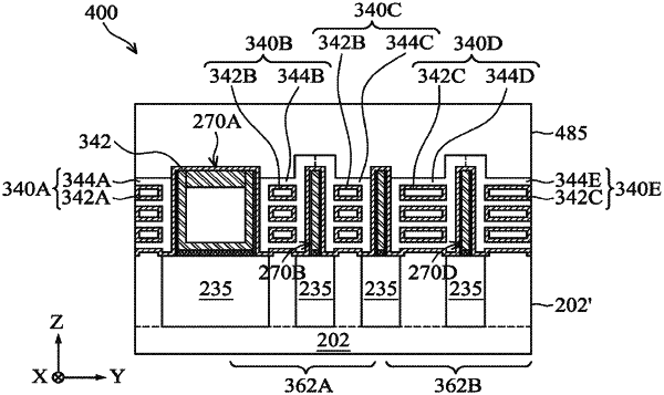
1. A device comprising:
a first multigate device having:
a first channel layer disposed between first source/drain features, and
a first metal gate that surrounds the first channel layer;
a second multigate device having:
a second channel layer disposed between second source/drain features, and
a second metal gate that surrounds the second channel layer; and
a gate isolation fin disposed between and separating the first metal gate and the second metal gate, wherein the gate isolation fin includes:
a first dielectric layer having a first dielectric constant, wherein the first dielectric layer has a bottom portion having a first thickness and sidewall portions having a second thickness, wherein the second thickness is less than the first thickness, and
a second dielectric layer disposed over the first dielectric layer, wherein the second dielectric layer has a second dielectric constant that is less than the first dielectric constant.
|