| CPC H01L 27/0738 (2013.01) [H01C 13/02 (2013.01); H01L 28/20 (2013.01)] | 20 Claims |
|
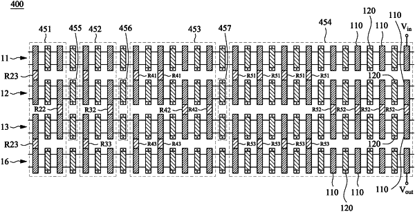
1. A trimmable resistor circuit, comprising:
first source/drain features arranged in a first row;
a first gate structure arranged in the first row and between the first source/drain features;
second source/drain features arranged in a second row;
a second gate structure arranged in the second row and between the second source/drain features, wherein the second gate structure is aligned with the first gate structure;
a first resistor disposed between the first row and the second row and comprising a first end directly connecting a first one of the first source/drain features and comprising a second end directly connecting a first one of the second source/drain features; and
a second resistor disposed between the first row and the second row and electrically connecting a second one of the first source/drain features and a second one of the second source/drain features.
|
|
9. A trimmable resistor circuit, comprising:
first source/drain features of a first transistor disposed in a first row;
second source/drain features disposed in the first row, wherein the second source/drain features are of a second transistor next to the first transistor;
third source/drain features of a third transistor disposed in a second row;
fourth source/drain features disposed in the second row, wherein the fourth source/drain features are of a fourth transistor next to the third transistor; and
a first resistor disposed between a first one of the first source/drain features of the first transistor and a first one of the third source/drain features of the third transistor, wherein the first resistor comprises a first end directly connecting the first one of the first source/drain features of the first transistor and a second end directly connecting the first one of the third source/drain features of the third transistor.
|
|
16. A trimmable resistor circuit, comprising:
first source/drain features disposed in a first row;
second source/drain features disposed in a second row;
third source/drain features disposed in a third row;
a first resistor disposed between a first one of the second source/drain features and a first one of the third source/drain features, wherein the first resistor comprises a first end directly connecting the first one of the second source/drain features and a second end directly connecting the first one of the third source/drain features; and
a second resistor disposed between a second one of the second source/drain features and a second one of the third source/drain features.
|