| CPC H01L 27/0288 (2013.01) [H01L 27/0255 (2013.01); H01L 27/0266 (2013.01); H02H 9/04 (2013.01)] | 19 Claims |
|
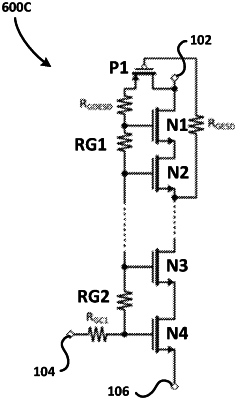
1. An RF switch device, comprising:
a plurality of transistors coupled in series forming an RF conductive current path;
a first resistive bias network forming a DC conductive bias path between gate nodes of the plurality of transistors; and
a first ESD bias component coupled between the RF conductive current path and the first resistive bias network, wherein the first ESD bias component is configured to provide a DC conductive path between the RF conductive current path of the RF switch device and the first resistive bias network during an ESD event, wherein the first ESD bias component comprises a switching transistor.
|