| CPC H01L 27/0262 (2013.01) [H01L 23/535 (2013.01); H01L 27/0255 (2013.01); H01L 29/0649 (2013.01); H01L 29/8611 (2013.01); H01L 29/866 (2013.01); H01L 29/87 (2013.01)] | 11 Claims |
|
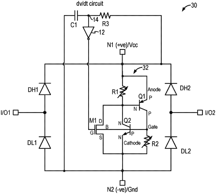
1. A bidirectional circuit transient voltage suppressing (TVS) protection circuit, comprising:
a first high-side diode having an anode coupled to a first protected node and a cathode coupled to a first node;
a first low-side diode having a cathode coupled to the first protected node and an anode coupled to a second node;
a second high-side diode having an anode coupled to a second protected node and a cathode coupled to the first node;
a second low-side diode having a cathode coupled to the second protected node and an anode coupled to the second node;
a clamp circuit comprising a MOS transistor integrated with a silicon controlled rectifier (SCR), the SCR having an anode coupled to the first node, a cathode coupled to the second node, and a gate terminal, and the MOS transistor having a first current terminal coupled to the anode of the SCR through a first variable resistor, and a second current terminal coupled to the second node, wherein the gate terminal of the SCR is coupled to the second node through a second variable resistor; and
a trigger circuit comprising a third resistor and a first capacitor connected in series between the first node and the second node, a third node between the third resistor and the first capacitor being coupled to a gate terminal of the MOS transistor and the gate terminal of the SCR,
wherein in response to a voltage applied to one of the protected nodes exceeding a first voltage level, the trigger circuit drives the MOS transistor to cause a current flow at the SCR to trigger an SCR action and the SCR clamps the voltage at the respective protected node at a clamping voltage.
|