US 11,990,466 B2
High voltage electrostatic devices
Kyong Jin Hwang, Singapore (SG); Robert J. Gauthier, Jr., Williston, VT (US); and Jie Zeng, Woodlands (SG)
Assigned to GLOBALFOUNDRIES Singapore Pte. Ltd., Singapore (SG)
Filed by GLOBALFOUNDRIES Singapore Pte. Ltd., Singapore (SG)
Filed on Oct. 14, 2021, as Appl. No. 17/501,270.
Prior Publication US 2023/0121127 A1, Apr. 20, 2023
Int. Cl. H01L 27/02 (2006.01); H01L 29/08 (2006.01); H01L 29/735 (2006.01); H02H 9/04 (2006.01)
CPC H01L 27/0262 (2013.01) [H01L 29/0821 (2013.01); H01L 29/735 (2013.01); H02H 9/046 (2013.01)] 20 Claims
OG exemplary drawing
 
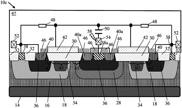
1. A structure comprising a high voltage NPN with polysilicon material bounded by silicide block layers located at collector and emitter regions, the polysilicon material being on an isolation structure located in a base region, the isolation structure extending between a collector and an emitter within a substrate, the polysilicon material extending to at least one of the collector and the emitter of a bipolar junction transistor (BJT), and the polysilicon material completely covering the base region of the BJT and an epitaxial semiconductor material between the collector and the base region.