| CPC H01L 27/0255 (2013.01) [H03K 17/6871 (2013.01)] | 11 Claims |
|
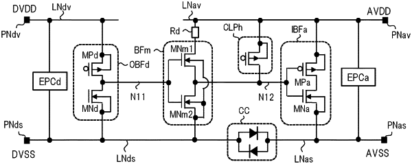
1. A semiconductor device including a first power supply system composed of a first high-potential side power supply and a first low-potential side power supply and a second power supply system composed of a second high-potential side power supply and a second low-potential side power supply, the semiconductor device comprising:
a first ESD protection circuit provided between the first high-potential side power supply and the first low-potential side power supply and configured to absorb an input surge;
a second ESD protection circuit provided between the second high-potential side power supply and the second low-potential side power supply and configured to absorb an input surge;
a coupling circuit including a bidirectional diode and configured to couple the first low-potential side power supply and the second low-potential side power supply;
a first transistor composed of an n-channel MOS transistor, having a drain coupled to the first high-potential side power supply, and having a back gate coupled to the second low-potential side power supply;
a first resistor element inserted in series between the drain of the first transistor and the first high-potential side power supply;
an input buffer to which a signal from the first transistor is input and which is coupled to the first high-potential side power supply and the first low-potential side power supply; and
a clamp circuit configured to clamp an input node of the input buffer,
wherein the clamp circuit is provided between the input node and the first high-potential side power supply and is not provided between the input node and the first low-potential side power supply.
|