| CPC H01L 25/50 (2013.01) [H01L 24/74 (2013.01); H01L 24/75 (2013.01); H01L 24/80 (2013.01); H01L 25/0652 (2013.01); H05K 13/0404 (2013.01); H01L 2224/80003 (2013.01); H01L 2224/80011 (2013.01); H01L 2224/80013 (2013.01); H01L 2224/80894 (2013.01)] | 13 Claims |
|
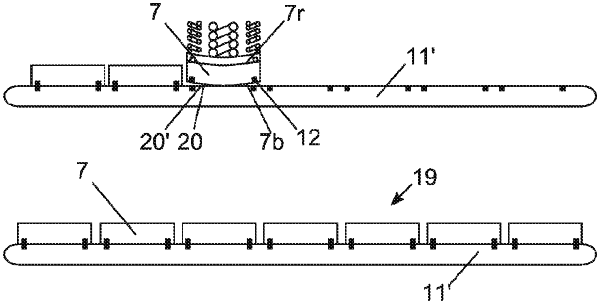
1. A device for bonding a plurality of chips onto a semiconductor substrate or onto further chips, the device comprising:
an ejector including a storage area for storing the plurality of chips; and
a bond head for positioning and aligning a chip of the plurality of chips, the bond head including
a first surface configured to couple to the chip of the plurality of chips that is to be bonded, and a second surface fixed to and disposed opposite the first surface,
a first spring element having a first spring constant, and
a second spring element having a second spring constant,
wherein the first spring constant is different from the second spring constant, and the first and second spring elements are coupled to the second surface.
|