US 11,990,462 B2
3D semiconductor device and structure with metal layers
Zvi Or-Bach, Haifa (IL); and Brian Cronquist, Klamath Falls, OR (US)
Assigned to Monolithic 3D Inc., Klamath Falls, OR (US)
Filed by Monolithic 3D Inc., Klamath Falls, OR (US)
Filed on Oct. 29, 2023, as Appl. No. 18/384,883.
Application 18/384,883 is a continuation in part of application No. 18/234,784, filed on Aug. 16, 2023, granted, now 11,923,374.
Application 18/234,784 is a continuation in part of application No. 18/111,300, filed on Feb. 17, 2023, granted, now 11,791,222, issued on Oct. 17, 2023.
Application 18/111,300 is a continuation in part of application No. 17/900,073, filed on Aug. 31, 2022, granted, now 11,631,667, issued on Apr. 18, 2023.
Application 17/900,073 is a continuation in part of application No. 17/843,957, filed on Jun. 18, 2022, granted, now 11,482,494, issued on Oct. 25, 2022.
Application 17/843,957 is a continuation in part of application No. 17/586,730, filed on Jan. 27, 2022, granted, now 11,398,569, issued on Jul. 26, 2022.
Application 17/586,730 is a continuation in part of application No. 17/472,667, filed on Sep. 12, 2021, granted, now 11,276,687, issued on Mar. 15, 2022.
Application 17/472,667 is a continuation in part of application No. 17/367,386, filed on Jul. 4, 2021, granted, now 11,145,657, issued on Oct. 12, 2021.
Application 17/367,386 is a continuation in part of application No. 17/169,432, filed on Feb. 6, 2021, granted, now 11,088,130, issued on Aug. 10, 2021.
Application 17/169,432 is a continuation in part of application No. 17/065,424, filed on Oct. 7, 2020, granted, now 10,950,581, issued on Mar. 16, 2021.
Application 17/065,424 is a continuation in part of application No. 15/482,787, filed on Apr. 9, 2017, granted, now 10,840,239, issued on Nov. 17, 2020.
Application 15/482,787 is a continuation in part of application No. 14/607,077, filed on Jan. 28, 2015, granted, now 9,640,531, issued on May 2, 2017.
Application 14/607,077 is a continuation in part of application No. 13/796,930, filed on Mar. 12, 2013, granted, now 8,994,404, issued on Mar. 31, 2015.
Claims priority of provisional application 62/042,229, filed on Aug. 26, 2014.
Claims priority of provisional application 62/035,565, filed on Aug. 11, 2014.
Claims priority of provisional application 62/022,498, filed on Jul. 9, 2014.
Claims priority of provisional application 61/932,617, filed on Jan. 28, 2014.
Prior Publication US 2024/0079401 A1, Mar. 7, 2024
This patent is subject to a terminal disclaimer.
Int. Cl. H01L 25/18 (2023.01); H01L 21/28 (2006.01); H01L 21/324 (2006.01); H01L 23/48 (2006.01); H01L 25/065 (2023.01); H01L 27/02 (2006.01); H01L 27/088 (2006.01); H01L 29/66 (2006.01); H01L 29/78 (2006.01)
CPC H01L 25/18 (2013.01) [H01L 21/28194 (2013.01); H01L 21/324 (2013.01); H01L 23/481 (2013.01); H01L 25/0657 (2013.01); H01L 27/0266 (2013.01); H01L 27/0886 (2013.01); H01L 29/66795 (2013.01); H01L 29/785 (2013.01); H01L 2225/06541 (2013.01)] 20 Claims
OG exemplary drawing
 
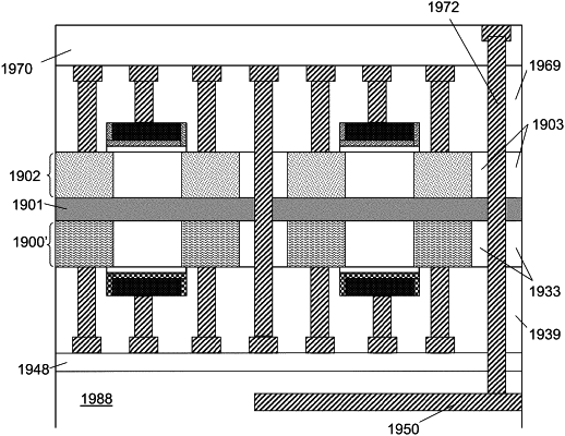
1. A semiconductor device, the device comprising:
a first silicon layer comprising a first single crystal silicon layer;
a plurality of first transistors each comprising a single-crystal channel;
a first metal layer disposed over said plurality of first transistors;
a second metal layer disposed over said first metal layer;
a third metal layer disposed over said second metal layer;
a second level comprising a plurality of second transistors, said second level is disposed over said third metal layer;
a third level comprising a plurality of third transistors, said third level is disposed over said second level;
a fourth metal layer disposed over said third level;
a fifth metal layer disposed over said fourth metal layer;
a via disposed through said second level,
wherein at least one of said plurality of second transistors comprises a metal gate,
wherein processing of said second transistors comprises use of Atomic Layer Deposition (“ALD”),
wherein an average thickness of said fifth metal layer is greater than an average thickness of said third metal layer by at least 50%; and
wherein at least one element within at least one of said plurality of second transistors has been processed independently of said plurality of third transistors.