| CPC H01L 25/18 (2013.01) [H01L 23/49822 (2013.01); H01L 23/49838 (2013.01); H01L 25/0652 (2013.01); H01L 25/50 (2013.01); H01L 2225/06513 (2013.01); H01L 2225/06541 (2013.01)] | 20 Claims |
|
1. An integrated circuit package comprising:
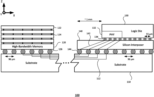
a multilayer substrate including a top surface layer and at least one lower layer separated from the top surface layer by a dielectric, the multilayer substrate configured to interface one or more high-bandwidth memory stacks with a logic die, wherein an upper surface of the one or more high-bandwidth memory stacks is configured to receive the multilayer substrate; and
a plurality of printed traces formed in the top surface layer and the at least one lower layer of the multilayer substrate, wherein the plurality of printed traces are configured to provide an interface between the logic die and the one or more high-bandwidth memory stacks.
|