| CPC H01L 25/167 (2013.01) [H01L 23/3121 (2013.01); H01L 23/5386 (2013.01); H01L 23/66 (2013.01); H01L 31/12 (2013.01)] | 13 Claims |
|
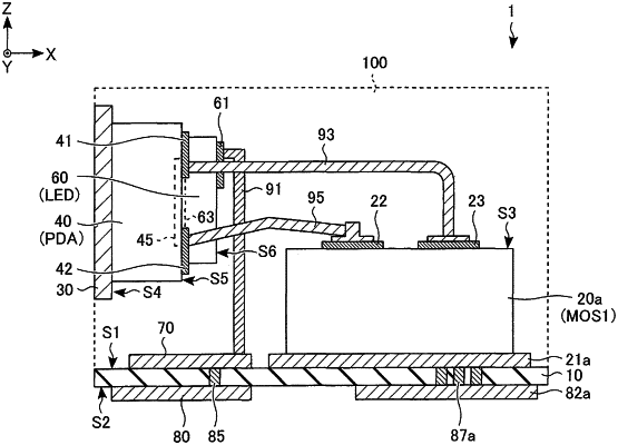
1. A semiconductor device comprising:
a substrate that has a first surface extending in a first direction and a second direction;
a first metal oxide semiconductor field effect transistor (MOSFET) that is provided on the first surface of the substrate;
a support base that is provided above the first surface of the substrate and extends in a third direction intersecting the first direction and the second direction;
a light receiving surface of a light receiving element that is oriented in the first direction; and
a light emitting element that is in contact with a third surface of the light receiving element facing the first direction.
|