| CPC H01L 25/167 (2013.01) [H01L 24/24 (2013.01); H01L 24/29 (2013.01); H01L 24/32 (2013.01); H01L 24/73 (2013.01); H01L 24/83 (2013.01); H01L 24/92 (2013.01); H01L 24/94 (2013.01); H01L 31/02008 (2013.01); H01L 31/1876 (2013.01); H01L 31/1892 (2013.01); H01L 24/82 (2013.01); H01L 31/1844 (2013.01); H01L 2224/24146 (2013.01); H01L 2224/245 (2013.01); H01L 2224/2919 (2013.01); H01L 2224/32145 (2013.01); H01L 2224/73217 (2013.01); H01L 2224/73267 (2013.01); H01L 2224/82106 (2013.01); H01L 2224/83203 (2013.01); H01L 2224/83862 (2013.01); H01L 2224/92144 (2013.01); H01L 2224/92244 (2013.01)] | 12 Claims |
|
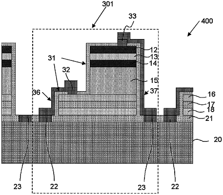
1. A method for producing an electronic device having a drive circuit comprising a solar cell structure, the method comprising the steps of:
obtaining a bonded wafer by bonding a first wafer having a plurality of independent solar cell structures comprising a compound semiconductor, the plurality of independent solar cell structures being formed on a starting substrate by epitaxial growth, and a second wafer having a plurality of independent drive circuits formed, so that the plurality of independent solar cell structures and the plurality of independent drive circuits are respectively superimposed;
wiring the bonded wafer so that an electric power can be supplied from the plurality of independent solar cell structures to the plurality of independent drive circuits respectively; and
producing the electronic device having the drive circuit comprising the solar cell structure by dicing the bonded wafer.
|