| CPC H01L 25/167 (2013.01) [H01L 33/62 (2013.01); G09G 3/32 (2013.01)] | 11 Claims |
|
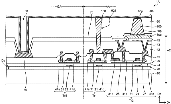
1. A display device comprising:
a substrate;
a plurality of pixels arrayed on the substrate;
an inorganic light-emitting element provided to each of the pixels;
an anode electrode electrically coupled to the inorganic light-emitting element;
a transistor provided on a first surface of the substrate;
coupling wiring that couples the anode electrode and the transistor;
an insulating planarization film that covers a side surface of the inorganic light-emitting element; and
a first heat transmitter disposed in a recess in the planarization film, wherein
the anode electrode protrudes from an inside to an outside of the inorganic light-emitting element in planar view from a normal direction of the substrate,
the anode electrode is disposed between an anode terminal of the inorganic light-emitting element and the coupling wiring that couples the anode electrode and the transistor, and the anode electrode, the anode terminal, and the coupling wiring all overlap with each other in planar view,
the area of the anode electrode is larger than the area of the inorganic light-emitting element in planar view, such that the anode electrode protrudes from an entire area of the inorganic light-emitting element to the outside of the inorganic light-emitting element in planar view,
temperature characteristics of the transistor are positive,
temperature characteristics of the inorganic light-emitting element are negative,
the temperature characteristics of the inorganic light-emitting element are opposite to the temperature characteristics of the transistor,
an upper end of the first heat transmitter is in contact with a cathode electrode, and
a lower end of the first heat transmitter is in contact with an insulating film constituting the transistor.
|