| CPC H01L 25/16 (2013.01) [H01L 23/4951 (2013.01); H01L 23/49562 (2013.01); H01L 23/49575 (2013.01); H01L 23/49589 (2013.01); H01L 24/06 (2013.01); H01L 24/38 (2013.01); H01L 24/41 (2013.01); H01L 24/49 (2013.01); H01L 24/73 (2013.01); H02M 1/08 (2013.01); H02M 3/003 (2021.05); H01L 24/40 (2013.01); H01L 24/48 (2013.01); H01L 2224/0603 (2013.01); H01L 2224/06051 (2013.01); H01L 2224/0615 (2013.01); H01L 2224/38 (2013.01); H01L 2224/4009 (2013.01); H01L 2224/40106 (2013.01); H01L 2224/40245 (2013.01); H01L 2224/41175 (2013.01); H01L 2224/48108 (2013.01); H01L 2224/48137 (2013.01); H01L 2224/48245 (2013.01); H01L 2224/4903 (2013.01); H01L 2224/49112 (2013.01); H01L 2224/4912 (2013.01); H01L 2224/49175 (2013.01); H01L 2224/73221 (2013.01); H01L 2924/10272 (2013.01); H01L 2924/10329 (2013.01); H01L 2924/1033 (2013.01); H01L 2924/1067 (2013.01); H01L 2924/13055 (2013.01); H01L 2924/13064 (2013.01); H01L 2924/13091 (2013.01)] | 25 Claims |
|
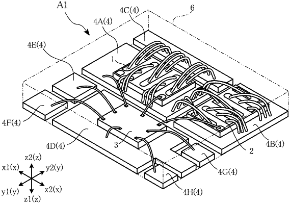
1. A semiconductor device comprising:
a conductive member including a first conductor, a second conductor and a third conductor that are spaced apart from each other;
a first semiconductor element having a first obverse surface on which a first drain electrode, a first source electrode and a first gate electrode are disposed; and
a second semiconductor element having a second obverse surface on which a second drain electrode, a second source electrode and a second gate electrode are disposed, wherein the first conductor is electrically connected to the first source electrode and the second drain electrode,
the second conductor is electrically connected to the second source electrode, and as viewed in a first direction orthogonal to the first obverse surface, the second conductor is adjacent to the first conductor in a second direction orthogonal to the first direction, and
the third conductor is electrically connected to the first drain electrode and is adjacent to each of the first conductor and the second conductor as viewed in the first direction.
|