| CPC H01L 25/0657 (2013.01) [H01L 24/02 (2013.01); H01L 25/0652 (2013.01); H01L 2224/02372 (2013.01); H01L 2225/06513 (2013.01); H01L 2225/06541 (2013.01); H01L 2225/06586 (2013.01); H01L 2225/06589 (2013.01); H01L 2924/18161 (2013.01)] | 18 Claims |
|
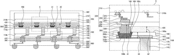
1. A semiconductor package comprising:
a first semiconductor chip comprising a semiconductor substrate and a redistribution pattern on a top surface of the semiconductor substrate, the redistribution pattern having a hole exposing an inner sidewall of the redistribution pattern;
a second semiconductor chip on a top surface of the first semiconductor chip; and
a bump structure disposed between the first semiconductor chip and the second semiconductor chip,
wherein the bump structure comprises a solder pattern filling the hole and being in direct contact with the inner sidewall of the redistribution pattern,
wherein a distance between the first and second semiconductor chips is less than a height of the bump structure,
wherein the distance between the first and second semiconductor chips ranges from about 3 μm to about 20 μm, and
wherein the height of the bump structure ranges from about 5 μm to about 30 μm.
|