| CPC H01L 25/0657 (2013.01) [H01L 23/49816 (2013.01); H01L 23/49822 (2013.01); H01L 23/49838 (2013.01); H01L 23/5226 (2013.01); H01L 23/5283 (2013.01); H01L 23/53209 (2013.01); H01L 23/5383 (2013.01); H01L 23/5386 (2013.01); H01L 24/08 (2013.01); H01L 29/42344 (2013.01); H10B 43/40 (2023.02); H01L 2224/08146 (2013.01); H01L 2225/06506 (2013.01); H01L 2225/0651 (2013.01); H01L 2225/06513 (2013.01); H01L 2225/06517 (2013.01); H01L 2225/06541 (2013.01); H01L 2225/06562 (2013.01); H01L 2924/1431 (2013.01); H01L 2924/1438 (2013.01); H10B 43/27 (2023.02); H10B 43/35 (2023.02)] | 19 Claims |
|
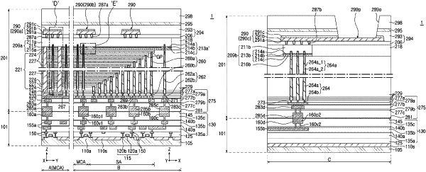
1. A semiconductor device comprising:
a substrate;
a peripheral circuit and first junction pads on the substrate;
a first insulating structure on the substrate and surrounding side surfaces of the first junction pads;
second junction pads contacting the first junction pads;
a second insulating structure on the first insulating structure and surrounding side surfaces of the second junction pads;
a passivation layer on the second insulating structure;
an upper insulating structure between the passivation layer and the second insulating structure;
a barrier capping layer between the upper insulating structure and the passivation layer, and including a material different from a material of the upper insulating structure and a material of the passivation layer;
conductive patterns spaced apart from each other in the upper insulating structure;
a first pattern structure between the upper insulating structure and the second insulating structure;
a stack structure between the second insulating structure and the first pattern structure, and including gate layers spaced apart from each other in a vertical direction; and
a vertical structure passing through the stack structure in the vertical direction, the vertical structure including a data storage structure and a channel layer; and
an input-output pad opening passing through the passivation layer and the barrier capping layer and extending into the upper insulating structure,
wherein the conductive patterns include a first conductive pattern and an input-output conductive pattern,
the input-output pad opening exposes a portion of the input-output conductive pattern,
the first conductive pattern overlaps the first pattern structure in the vertical direction, and
the input-output conductive pattern does not overlap the first pattern structure in the vertical direction,
each of the conductive patterns includes a first conductive layer, a second conductive layer, and a third conductive layer sequentially stacked,
a thickness of the second conductive layer is greater than a thickness of each of the first conductive layer and the third conductive layer, and
the input-output pad opening passes through the third conductive layer of the input-output conductive pattern and exposes the second conductive layer of the input-output conductive pattern.
|