| CPC H01L 25/0657 (2013.01) [H01L 25/105 (2013.01); H01L 25/50 (2013.01); H01L 2225/0651 (2013.01); H01L 2225/06562 (2013.01); H01L 2225/06586 (2013.01); H01L 2225/1041 (2013.01); H01L 2225/1058 (2013.01)] | 10 Claims |
|
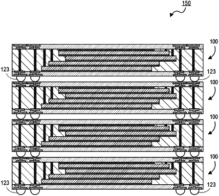
1. A package on package (PoP) system, comprising:
a first package on a second package;
an electronic component on the first package; and
a plurality of first solder balls between the first package and the second package, wherein the plurality of first solder balls couples the first package to the second package, and wherein each of the first package and the second package includes
a first redistribution layer;
a stack of dies on the first redistribution layer;
a second redistribution layer over the stack of dies and the first redistribution layer;
a plurality of interconnects, wherein first ones of the plurality of interconnects extend substantially vertical from a top surface of the first redistribution layer to a bottom surface of the second redistribution layer, wherein the first ones of the plurality of interconnects are laterally spaced apart from the stack of dies, wherein second ones of the plurality of interconnects extend from a corresponding one of the stack of dies to the bottom surface of the redistribution layer, and wherein a first portion of the second ones of the plurality of interconnects are adjacent to a first side of the stack of dies, and a second portion of the second ones of the plurality of interconnects are adjacent to a second side of the stack of dies, the second side laterally opposite to the first side;
a mold layer between the first redistribution layer and the second redistribution layer, a portion of the mold layer vertically between an uppermost surface of the stack of dies and the bottom surface of the second redistribution layer, wherein the first ones of the plurality of interconnects extending from the first redistribution layer to the second redistribution layer are in direct contact with the mold layer, and wherein the first ones of the plurality of interconnects extending from the first redistribution layer to the second redistribution layer have an uppermost surface at same level as an uppermost surface of the mold layer,
a substrate; and
a third package on a fourth package, wherein a plurality of second solder balls couples the second package onto the third package, wherein a plurality of third solder balls couples the third package onto the fourth package, wherein a plurality of fourth solder balls couples the fourth package onto the substrate, wherein the first, second, third, and fourth packages are disposed vertically on top each other substantially with no offset, and wherein each of the third package and the fourth package includes
a first redistribution layer;
a stack of dies on the first redistribution layer;
a second redistribution layer over the stack of dies and the first redistribution layer; and
a plurality of interconnects coupled to the stack of dies and the first and second redistribution layers, wherein the plurality of interconnects extend substantially vertical from a top surface of the first redistribution layer to a bottom surface of the second redistribution layer.
|